 ®
®
More Digital Logic Gates
Kennesaw State University
Copyright © 2000, 2002 by Bob Brown
A Note on Terminology
Boolean algebra is a two-valued algebra. Variables and expressions can be either true
or false. When we implement Boolean functions with electronic circuits, we choose the
binary values one and zero to represent true and false respectively. In
this Web Lecture,
one, 1, and true all mean the same thing. Zero, 0, and false are equivalent to each
other.
Computational Completeness
We ended the previous Web lecture with the bold statement that NAND and NOR are computationally complete. By that we mean that any Boolean function can be represented using only NAND or only NOR. That means that any digital logic circuit can be implemented using only NAND or only NOR. This property is sometimes called computational completeness or functional completeness.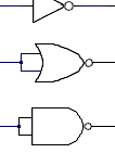 |
|||||
| Figure 1. Three represenations of the NOT function. A. The standard symbol. B.Using a NOR gate. C. Using a NAND gate. | |||||
We will not prove the completeness of NAND and NOR but we will demonstrate it by showing how other gates can be constructed using only NAND or only NOR.
Figure 1 shows three ways to compute the NOT function. The first is the inverting amplifier from the previous Web lecture. This is the standard symbol for NOT. Using this symbol hides the details of the implementation from us. This is yet another example of abstraction. Experiment by clicking the pushbutton. The output of the NOT function is the opposite, or inverse of the input.
The second part of Figure 1 shows a NOR with both inputs connected to the pushbutton. You will find by experimenting that this circuit also computes the NOT function. If you refer to the truth table for NOR in the previous lecture, you will see that the output of a NOR gate is true only when neither input is true. Because the two inputs are connected, only 0 0 or 1 1 can be presented to the NOR gate. From the truth table we see that an input of 1 1 generates an output of 0 and an input of 0 0 generates an output of 1. In other words, this circuit computes the NOT function, as you have already seen by experiment.
It may surprise you to find that the third circuit of Figure 1 also computes the NOT function. It is identical to the second circuit, but the gate is a NAND gate. A moment's thought, or a peek at the truth table for the NAND gate will show you that an input of 0 0 results in an output of 1, and an input of 1 1 results in an output of 0.
From this point forward, we will use the triangle symbol with inversion bubble to represent
the NOT function regardless of how that function is implemented.
The OR Function
 |
 |
||||||||
 |
|||||||||
| Figure 2. Three implementations of the OR function. A. The standard symbol. B.Using NOR gates. C. Using NAND gates. | |||||||||
| A | B | X | |||
|---|---|---|---|---|---|
| 0 | 0 | 0 | |||
| 0 | 1 | 1 | |||
| 1 | 0 | 1 | |||
| 1 | 1 | 1 |
Table 1 gives the truth table for the OR function.The function is true whenever at least one of the inputs is true. Examination of the table shows that the output of the OR function is the complement of the output of the NOR function. Figure 2B is a circuit with a NOR and a NOT gate, or inverter. This circuit also computes the OR function. You can verify this by experimenting with the circuit. An extra LED in the middle of the circuit shows the output of the NOR gate before being complemented by the inverter.
Abstraction keeps the details of the implementation of the inverter hidden, but it could very well be implemented using a NOR as shown in Figure 1. In that case, the OR function would be implemented using only NOR gates.
It probably didn't surprise you to find that OR can be implemented using a NOR gate and an inverter. Figure 2C shows a NAND gate with both inputs inverted. This circuit also computes the OR function. Try it and see. You can observe the intermediate values via LEDs conected to the inverter outputs. If the inverters were implemented as NAND gates, the entire function can be implemented using only NAND gates.
DeMorgan's
Theorem, which we will study when we take up Boolean algebra, describes
the relationship among AND, OR, and inversion or complementation.
The AND Function
 |
 |
||||||||
 |
|||||||||
| Figure 3. Three implementations of the AND function. A. The standard symbol. B.Using NAND gates. C. Using NOR gates. | |||||||||
| A | B | X | |||
|---|---|---|---|---|---|
| 0 | 0 | 0 | |||
| 0 | 1 | 0 | |||
| 1 | 0 | 0 | |||
| 1 | 1 | 1 |
Since the truth table for AND is the inverse of the truth table for NAND, it makes sense that a NAND and an inverter (which could also be a NAND gate) can compute the AND function.
Figure 3C shows how the AND function can be computed using a
NOR gate and inverters. The inverters could also be made from
NOR gates. Once again DeMorgan's Theorem can be used to prove
that the circuit of Figure 3C computes the AND function.
The Exclusive-OR Function
| Figure 4. The XOR, or exclusive-or gate. This gate computes the "odd" function; the output is true if the number of true inputs is odd. | |||||
| A | B | X | |||
|---|---|---|---|---|---|
| 0 | 0 | 0 | |||
| 0 | 1 | 1 | |||
| 1 | 0 | 1 | |||
| 1 | 1 | 0 |
There are a couple of interesting things about exclusive-or. One is that if a bit is XORed with itself, the result is zero regardless of whether the original bit was zero or one. This means that a register can be cleared to all zeros by XORing the contents of the register with itself.
As with other gates, the XOR can have more than two inputs. The output of XOR is true when the number of one-inputs is odd. This makes useful in generating parity bits. Since the output is one when the number of one-inputs is odd, the ouptut can be used directly as the parity bit if even parity is desired.
For the previous gates, circuit equivalence to NAND and
NOR has been shown. It is omitted this time. See whether you
can design an XOR circuit using AND,
OR, and NOT.
Why So Many Gates?
If any digital logic circuit can be implemented using only NAND or only NOR, you may be wondering why we bother with all the other symbols. Once again, the answer is abstraction. We want our digital logic diagrams to be clear, so we want different symbols for each function.Only when it is time to design the physical layout of an integrated circuit do engineers apply the principle of circuit equivalence to convert the gates in the logic diagram to the gates required by the particular fabrication process to be used.
Table of Contents![]() Previous: Transistors and Digital Logic
Gates
Previous: Transistors and Digital Logic
Gates![]() Next: Designing Digital Logic
Circuits
Next: Designing Digital Logic
Circuits
Originally published: 2000-09-04
Copyright © by Bob Brown. Some rights reserved.
This work is licensed under a Creative Commons Attribution-NonCommercial-ShareAlike 3.0 Unported License.
Last updated: 2017-12-03 12:50